
SEMICONDUCTOR PROCESS APPLICATIONS
Acmewin Aibo Dry Asher platforms support photoresist strip, de-scum, light plasma treatment, residue-removal and plasma-cleaning applications for semiconductor manufacturing.
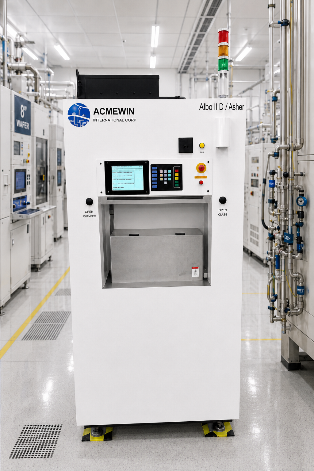
Applications Overview
Aibo Dry Asher process applications are reviewed according to wafer size, material stack, residue condition and downstream process requirements.
Photoresist Strip
Removes photoresist and organic material after lithography, implantation or etch processing.
De-scum
Removes thin resist residue after lithography development and before downstream processing.
Lite Etch
Uses controlled plasma exposure for light surface treatment and process development review.
Plasma Clean
Supports organic contamination treatment and selected process residue review.
Residues After Strip
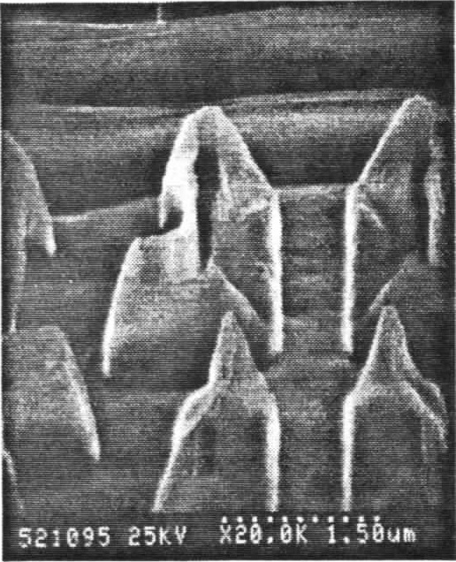
Anisotropic etching and high-dose ion implantation can form complex compounds that may remain after conventional oxygen-only photoresist ashing.
- Carbonized photoresist after high-dose implantation
- Poly-etch sidewall polymer
- Nitride-etch residue
- Metal-etch stringers
- Via-etch cone- or crown-like residue
- Organic contamination after conventional strip
Application details and process parameters are reviewed according to wafer structure, material stack and project requirements.
Residue-Removal Process Capability
Post-Poly Etch
Conventional Photoresist Strip
Sidewall polymer residue may remain after conventional photoresist strip.
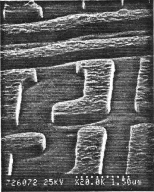
Aibo Residue-Removal Process
Reference SEM image showing improved sidewall polymer removal after an optimized residue-removal process sequence.
Post-Nitride Etch
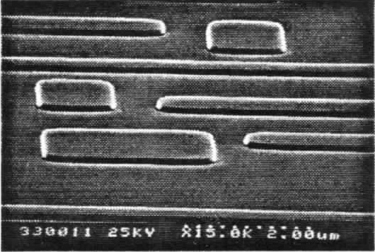
Post-Nitride Etch SEM 01
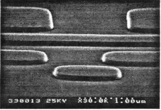
Post-Nitride Etch SEM 02
Post-Nitride Etch Residue-Removal Reference: Reference SEM images illustrating residue-removal process capability following plasma strip and selected post-treatment.
Example flow: O2 Plasma Strip -> Optional Residue-Removal Treatment -> DI Rinse.
Actual chemistry and process settings depend on device structure, material stack and application requirements.
Reference SEM images illustrating residue-removal process capability. Actual results depend on wafer structure, material stack, process sequence and recipe configuration.
Process Challenge to Aibo Approach
Configurable plasma strip and residue-removal sequence.
Multi-step strip and residue-removal capability.
Plasma strip with optional residue-removal treatment.
Application-specific plasma and post-treatment review.
Application Advantages
Low-Damage Plasma Processing
Plasma architecture designed to minimize electrical charge risk.
Configurable Residue-Removal Sequences
Process steps can be reviewed according to material stack, wafer structure and application requirements.
Multi-Application Platform
Common platform support for strip, de-scum, lite etch and plasma clean.
Process Monitoring
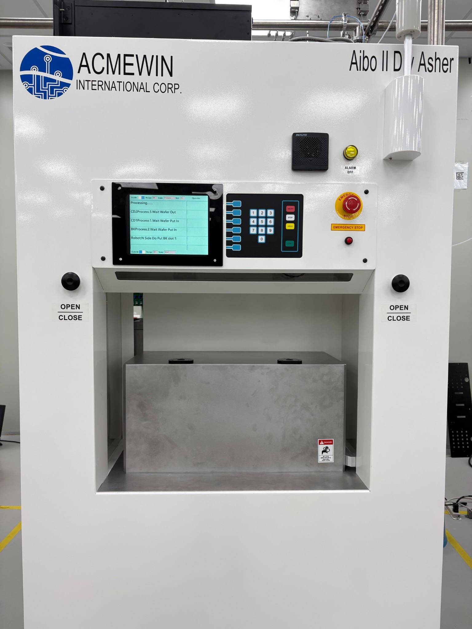
Recipe, trend, alarm and history functions support equipment operation and process review.
Process Control and Monitoring
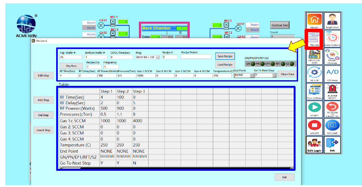
Recipe Management
Recipe workflows support controlled process setup and operating review.
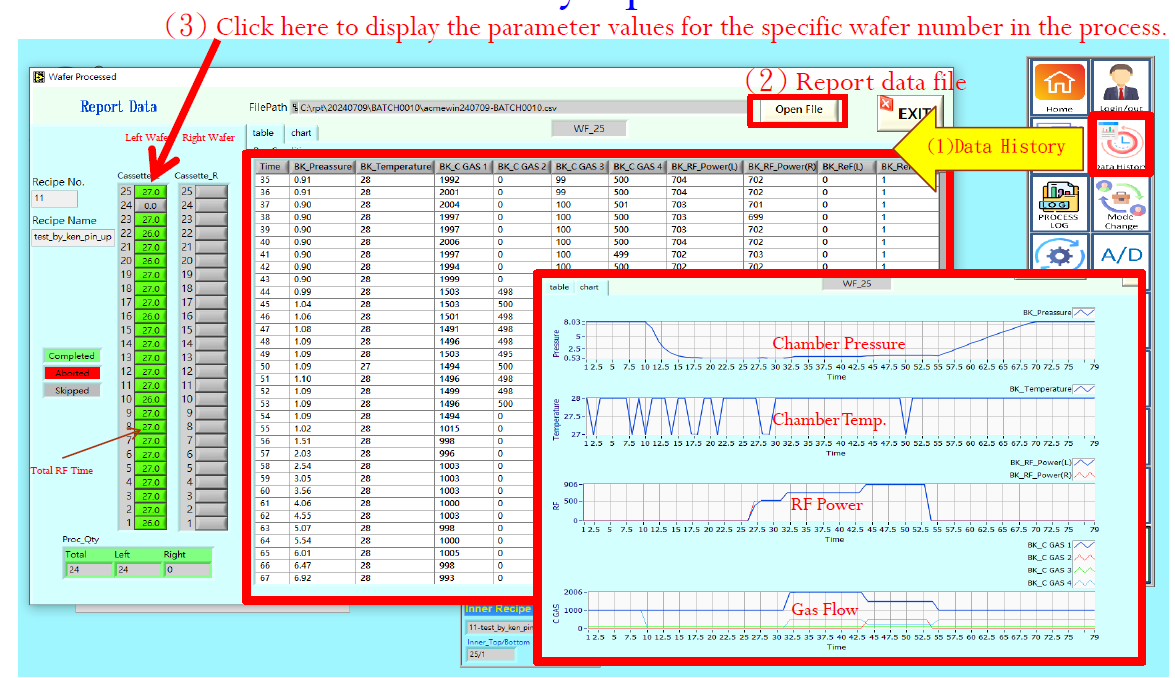
Process Trend Monitoring
Trend views support process and equipment status review.
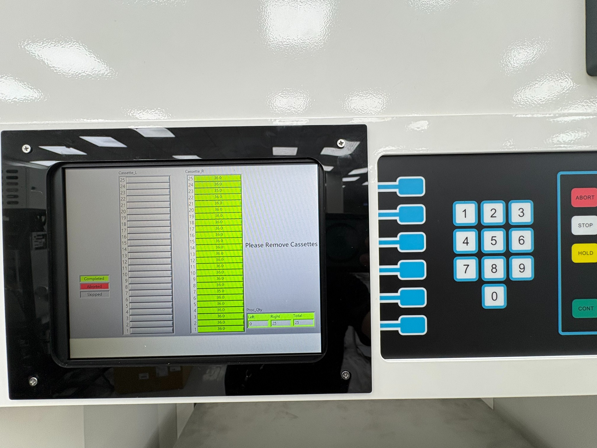
Alarm and Event History
Alarm and event information supports troubleshooting and maintenance planning.
Endpoint Monitoring
Endpoint requirements are reviewed according to process scope and system configuration.
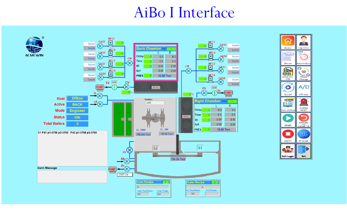
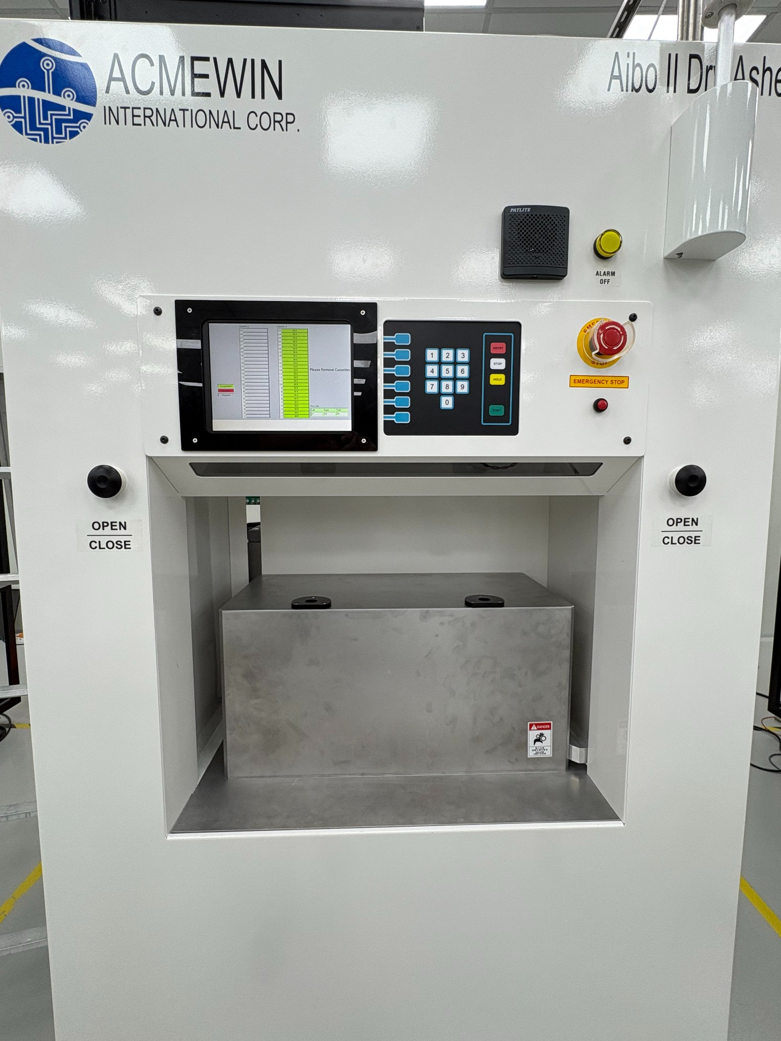
Equipment Status
Equipment status views support operator workflow and service response.
Application-to-Platform Guide
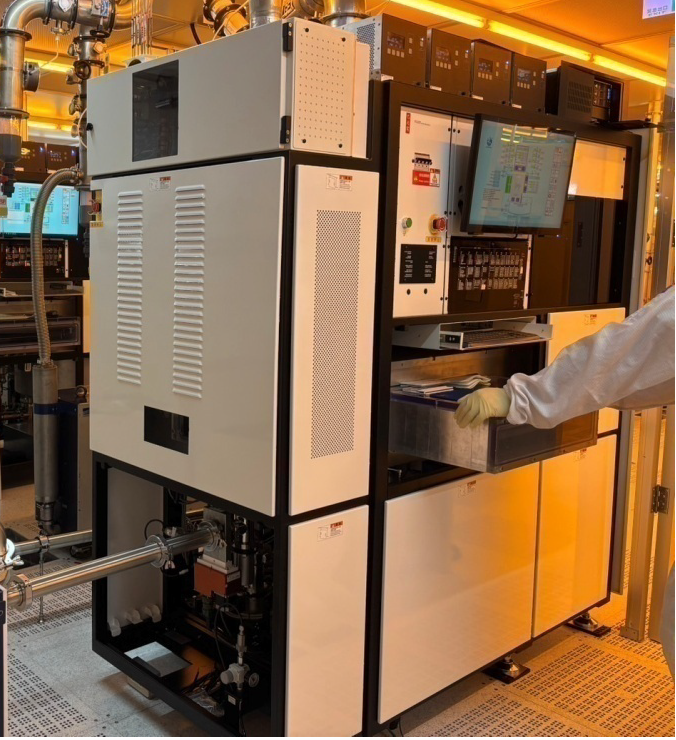
Aibo I Dry Asher
Compact dry asher and legacy equipment upgrade solution.
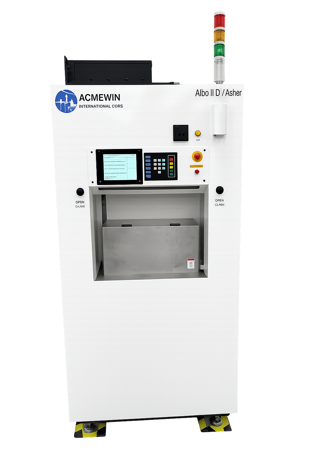
Aibo II Dry Asher
4-8 inch multi-application dry asher platform for strip, de-scum, lite etch and plasma clean.
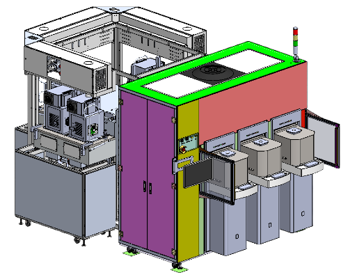
Aibo III Dry Asher
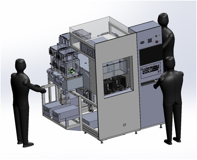
12-inch conceptual triple process module platform. Conceptual Design / 3D Layout Rendering.
Related Solutions
Technology
Review plasma, RF, vacuum and automation architecture.
Acmewin Innovation
Explore RF, pressure-control and wafer-handling innovation summaries.
Aibo I Upgrade Solution
Review legacy equipment upgrade and HMI modernization paths.
Aspen2 Services
Review lifecycle support for used equipment, parts, repair and upgrades.
Discuss Your Dry Asher Application
Provide wafer size, process type, material structure, current equipment and required capacity for application review.